Placed and routed for you
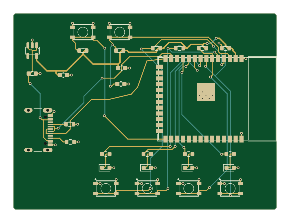
CELUS stops at the schematic. siliXon places and routes the board in the same flow.

 Try siliXon
CELUS turns your requirements, a sketch or a block diagram into a schematic and a BOM built from validated circuit modules, which is genuinely useful. Then it politely hands you over to your EDA tool, where placement, routing and the fab package are still your job. siliXon does not stop at the schematic: from one plain-English description it picks the parts, draws the circuit, places and routes the board and exports Gerbers, drill files, a BOM and pick-and-place data.
Free plan. Runs in your browser.
Who leads on what matters when you want a board.


siliXon: A plain-English description
CELUS: Text, a sketch or a block diagram
CELUS leads.siliXon: None
CELUS: PCB layout in your EDA tool
siliXon leads.siliXon: siliXon; you steer and edit
CELUS: Its AI up to the schematic; you lay out
siliXon leads.siliXon: An editable PCB and fab files
CELUS: A schematic, BOM and EDA project
siliXon leads.siliXon: Minutes
CELUS: No PCB of its own
siliXon leads.siliXon: Up to 4 layers
CELUS: Set by your EDA tool
Even.siliXon: None
CELUS: Place and route it in your EDA tool
siliXon leads.Verdict
Choose siliXon to get a finished, routed board from one tool.
Choose CELUS to generate a schematic and BOM for your existing EDA workflow.
siliXon todaysiliXon is in early beta and builds two- and four-layer, mostly digital boards. Review every design before fabrication.
Where CELUS is strongerValidated circuit modules from manufacturer app notes, supply data on every part, sketch and image input, and handoff to professional EDA tools.
Time to a prototype
From an idea to a board you can send to a fab, on one scale from zero. Estimates for someone new to each tool.
CELUS stops at the schematic. siliXon places and routes the board in the same flow.
No handoff to Altium, KiCad or Fusion to finish the layout. It all runs in the browser.
Export Gerbers, drill, BOM and pick-and-place data straight from siliXon.
| Feature | | |
|---|---|---|
| Starting point | A plain-English description | Text, sketch or block diagram |
| AI generation | Generates the whole board | Block diagram, schematic and BOM |
| PCB layout | Editable in 2D and 3D | No; you lay out in your EDA tool |
| Copper layers | Up to 4 | Set by your EDA tool |
| Part selection | Real, available parts picked for you | Validated modules with supply data |
| Design checks | Connectivity and manufacturing checks | Interface compatibility checks |
| Fab outputs | Gerbers, drill, BOM and pick-and-place | EDA project export; no Gerbers |
| Firmware | Programmable over USB, with flashing steps | Not stated |
| Layout prep | None; answer a few questions | Hand off to your EDA tool for layout |
| Runs in | Browser | Browser |
siliXon is in early beta and builds two- and four-layer, mostly digital boards. Review every design before fabrication.
So far creating my first project for 10 min - onboarding seems quite smooth
I like the self validation and how it explains everything too, makes it easier for me to quickly cross reference and learn on the go
Response is very meaningful, I like how it asks you questions to verify and gives you the options to choose the answers with the recommended on the one it thinks is a better option
Good so far. It is helpful and gives me advice
I have to say I love the UI and UX, the front end is really fun to interact with, with the little dynamic touches etc
Super helpful and easy to use
Really good actually better than Flux ai
 siliXon vs KiCadFree, open-source desktop EDA for schematics and PCB layout
 siliXon vs Altium DesignerProfessional EDA for complex, multi-layer production boards
 siliXon vs SchematikAI that turns a prompt into Arduino, ESP32 and Pico projects
 siliXon vs Blueprint.ioAI build plans with parts, wiring and assembly steps
 siliXon vs Flux.aiBrowser ECAD with an AI agent that designs alongside you
 siliXon vs DiodeAI-assisted board design service, from spec to production
 siliXon vs QuilterAI placement and routing from your finished schematic
 siliXon vs SnapMagicAI copilot for Altium, built on the SnapEDA parts library
 siliXon vs atopileCode-native electronics design, with an agent in the browser
 siliXon vs tscircuitOpen-source framework for designing PCBs in TypeScript
No. Its docs tell you to place, route and finish the layout in your EDA tool.
A PDF report, CSV BOMs and a project package for Altium, Fusion/Eagle or KiCad, with footprints still to be placed.
Community accounts are free, but their projects are public. Professional accounts are a paid annual subscription.
When you already lay out in Altium, Cadence, Siemens or KiCad and want AI help up to the schematic and BOM.